Etched copper
A simple method for making printed circuit boards for electronic applications is to take a copper-clad board and coat it with an ultraviolet-sensitive photoresist. A pattern of conducting tracks can be imaged onto the board with an ultraviolet light. When developed, this leaves the photoresist where the copper is required. The board is then placed in acid. This etches away the exposed copper, leaving the required track pattern.
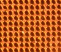
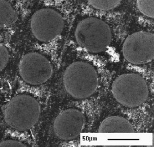
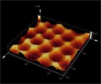
Rather than creating tracks, we can use the same etching process to create craters in a copper clad board. If we etch the craters until they join up, they create a landscape of sharp pinnacles, as in the centre image below. The method allows the roughness of the surface to be varied in a controlled manner. When we apply a hydrophobic coating to the etched surface, the contact angle increases with increasing roughness, to the point where the surface becomes superhydrophobic. Read more about the process in the publication below.
Publication
Wetting and wetting transitions on copper-based super-hydrophobic surfaces N.J. Shirtcliffe, G. McHale, M.I. Newton, G. Chabrol and C.C. Perry, Langmuir 21 (2005) 937-943